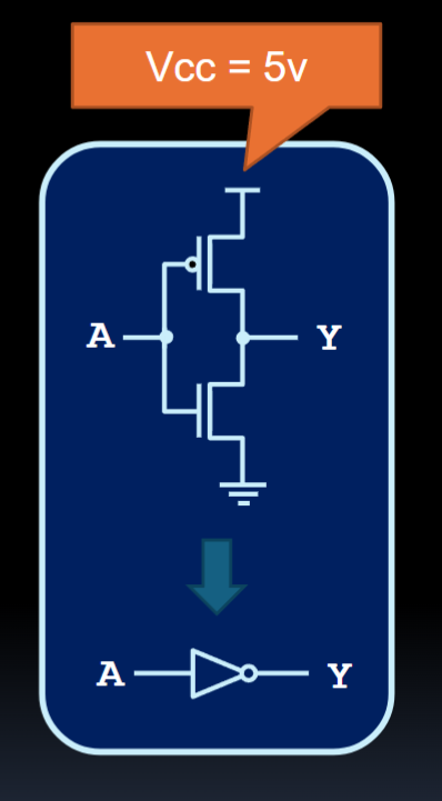
Refer to Circuits with Physical Switches for the first AND gate via physical switches. ALL digital logic gates (AND, OR, NOT, etc.) are created by a combination of nMOS and pMOS Transistors (pMOS and nMOS)!
The below is a CMOS circuit
is the top point; the ground is the bottom point (ignore the battery!)

Example: NAND gate
NAND gates OP
- They are the cheapest to make
- They can implement every other kind of gate
- Reference the truth table. See what kind of output is easier / has less entries.
- For a NAND gate, true can occur in 3 ways; false can occur in only 1 way. Let’s work with the output Y and ground
- Create the appropriate half of the circuit from there!
- false occurs when A and B are true. And = series, so we will have two pMOS transistors in series going into ground.
- Create the other half by inverting the solved half
- For the top, the series becomes parallel and the pMOS transistors become nMOS ones.
Do the rest! Refer to slide 46. You can do these as regular circuits or CMOS (or Transistor) Circuits