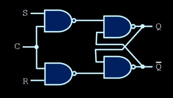
 “C” is usually connected to a “clock signal” (there are cases its connected to other weird things or even just a button for trivial circuits!)
- When C is 1, the NANDs work as inverters (allows normal operations)
- When C is 0, the NANDs are blocked (the out is 1)
- The reason why C=0 retains the previous information is that the “second level” of NANDs also become inverters.
- goes into the NAND going into Q. Whatever was is just inverted, but that was the same value as before.
Observe the second half is basically a Not S not R latch but the NANDs act as inverters when clocked, which is why this is actually a Clocked SR latch
Clocked = has a clock signal. Depending on the clock, the thingy is either operating or preserving what it had before
Final behaviour chart
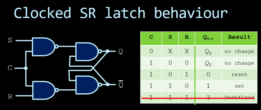
- When C is 0, nothing changes
- Then when C is 1, there are the 4 permutations of S and R to go through. But S=R=1 is still a pain. We need a solution!