The Control Unit
It receives the “opcode first. This determines which “branch” to take from start state (there are tens of them for add, load, store, etc.!)
The next opcode needs to be ready before the branch terminates and the FSM returns to the start state
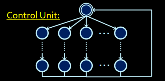
- The control unit does a loop!
The opcode (from the current instruction) is used to send Signals to the rest of the processor. The control unit has an FSM that can take many clock cycles for a single instruction. (the control unit sends out different signals on each clock)
- Chaos, chaos!
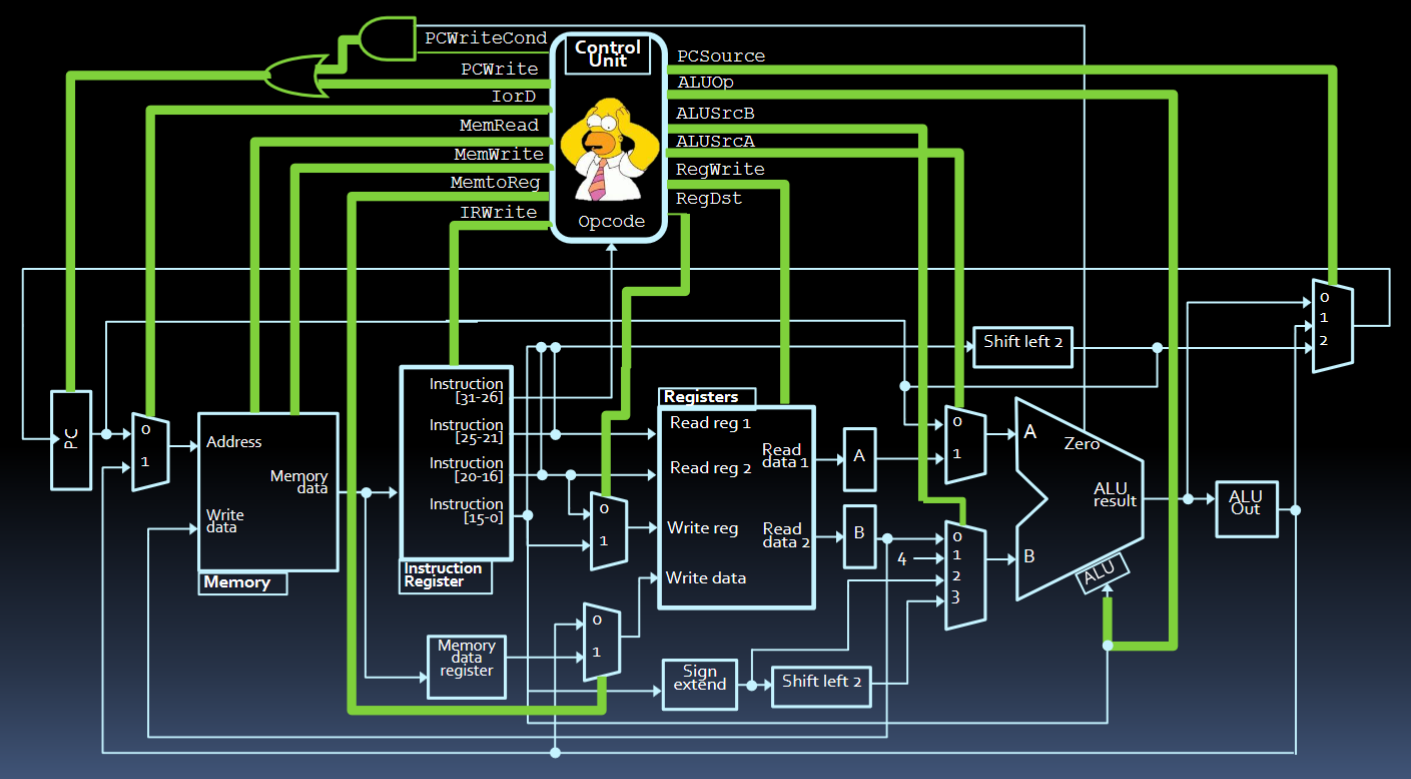
The PC is updated after every instruction ends. After that, the next instruction is fetched!
- However if we jump to another instruction (i.e. we don’t just +4 like always), we calculate the new PC value!
add s0 $zero
for the mux (0,1,2) that returns to PC, the ALU out is to delay the return by 1 cycle (why? Well we’ll find out soon)
The ALU instruction also takes from the “function” of the current instrctiontodo Then why is that from bits 15-0. Those are not the bits for the function at al!!!! Unless I am being dumb. I also dunno if they’re “combined” with ALUOp or if it’s either or (prolly combined tho)
- WAit no i think the diagram is just messed up (notice there’s no “dot” that splits the wire coming from 15-0)
Memory Data Register again is used for that 1 cycle delay ) Shift left 2 is required for operations that use offsets
If we aren’t writing, it should always be 0. Otherwise it’s 1. Never “don’t care”